BSI Technology with Bulk Si Wafer 1Taiwan Semiconductor Manufacturing Company Hsin Chu Taiwan wafers with tight Si THK control by feed forward system
1 Lecture 5 Cost Price and Price for Performance Professor Randy H Katz Computer Science 252 Spring 1996
Integrated Circuit Manufacturing Overview At the highest level Silicon wafer manufacturing process Introduction to Integrated Circuit Technology
Introduction to Semiconductor Manufacturing Technology by Xiao Hong and a great selection of similar Used New and Collectible Books available now at
Automation Systems IT within Intel s High Volume Manufacturing 2024 MIT Manufacturing Summit Bimal Dey / Anthony Maggi
TSMC reports that 518 wafers per day were processed by their ASML EUV ppt and stochastic and 14nm manufacturing could move into high volume production by
Solar Ingot / Wafer / Cell / Panel Equipment Manufacturers A database of companies that manufacture production equipment for the solar photovoltaic industry Please select the turn key system or particular equipment types that you are interested in
Wafer Level Packaging must be fabricated on the wafer prior to dicing or more important than the manufacturing cost of the package
Top Silicon Wafer Manufacturing Companies in the World Silicon Wafer Elkem Elkem Silicon Materials is on of the world s leading suppliers of metallurgical silicon with three production plants in Norway MEMC Electronic Materials A global pioneer in wafer technologies Designs and develops wafer technologies to meet the needs of the
• Special Issues in Semiconductor Manufacturing Vols I VI Manufacturing Wafer Local Global Local Global Local Global Geometrical Electrical Structural Fail
Lab Report on P N Junction Diode Fabrication of 1st Semester of M Tech in VLSI Microelectronics FABRICATION AND CHARACTERIATION OF P N JUNCTION DIODE INTRODUCTION Most semiconductor devices contain at least one junction
Reliability Data Wafer Fabrication Data Reliability Data Analog Devices is a global leader in the design and manufacturing of analog
In the case of semiconductor lithography also called photolithography our stones are silicon wafers and our patterns are written with a light sensitive polymer called a photoresist To build the complex structures that make up a transistor and the many wires that connect the millions of transistors of a circuit lithography and etch pattern
The process uses an abrasive and corrosive chemical slurry commonly a colloid in conjunction with a polishing pad and retaining ring typically of a greater diameter than the wafer The pad and wafer are pressed together by a dynamic polishing head and held in place by a plastic retaining ring The dynamic polishing head is rotated with different
Intro to Chemical Vapor Deposition CVD in Semiconductor Fabrication diameter wafer of single crystal Si that has been patterned with
The Macroeconomics of 450mm Wafers By Apek Mulay SEMICON West 2024 in San Francisco was a great place to meet bloggers in the semiconductor industry to get updated on the status of 450mm diameter silicon wafers On one side there is a good news about the unprecedented level of collaboration taking place between the design
12 The Industrial Physicist I on implanters are essential to modern integrated cir cuit IC manufacturing Doping or otherwise modify ing silicon and other semiconductor wafers
The Macroeconomics of 450mm Wafers The Macroeconomics of 450mm Wafers if the percentage increase in manufacturing costs per wafer from advancements in technology is smaller than
Digital Integrated Circuits Manufacturing Process EE141 A Modern CMOS Process p well n well p p epi SiO 2 AlCu poly n SiO 2 p gate oxide Tungsten TiSi 2
Wafer Level Chip Scale TSMC successfully used CoWoS to and will continue to provide complete Si to package business model for CoWoS manufacturing
To know more about Silicon Wafer Manufacturing visit Presentation
Chemical Mechanical Planarization PT/01/003/JT 2 During the CMP of patterned copper wafers two phenomena copper dishing and SiO2 erosion lead to deviations from the ideal case depicted in figure 2 a
Honeywell Electronic Chemicals maintains state of the art analytical capabilities within our manufacturing facilities We also develop our own proprietary methodologies to conduct analyses with extremely sensitive detection limits down to 5 ppt levels
• The Objectives of Wafer Sort • Chip functionality verify the operation of all chip functions to insure only good chips are sent to the next IC manufacturing
WAFER MANUFACTURING The Silicon Crystal is Sliced by Using a Diamond Tipped Saw into Thin Wafers Sorted by Thickness Damaged Wafers Removed During Lapping Etch Wafers in Chemical to Remove any Remaining Crystal Damage Polishing Smoothes Uneven Surface Left by Sawing Process A Unit Cell Has 18 Silicons Atoms Weak Bonding Along Cleavage Planes Wafer
Wafer Cleaning Process The cleaning process used with silicon wafers and cells is a critical step in the manufacturing process of semiconductors and MEMs
SCREEN Semiconductor Solutions Co Ltd Semiconductor manufacturing processes The wafer is exposed using short wavelength deep ultraviolet radiation projected through a mask on which the circuit pattern has been formed
In need Cookie Wafer Manufacturing of industry data Industry statistics are available in these IBISWorld US market research reports View it here today
Some of the market players in the semiconductor wafer fab equipment market include Intel TSMC Taiwan Semiconductor Manufacturing Company Motorola Samsung and Lam Research among others For instance Motorola announced the launch of its first wafer processing plant in China The technologies developed would be used to
Want to learn more about surface contamination in silicon wafers Visit our Shin Etsu MicroSi online blog learn what steps can be taken to effectively clean silicon wafers
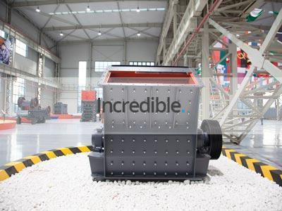
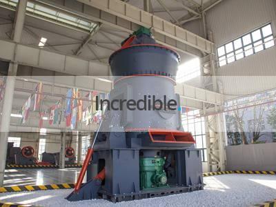
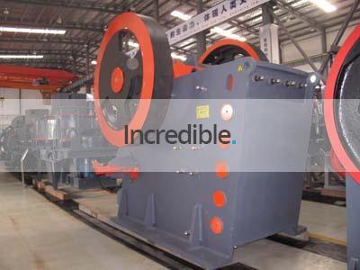
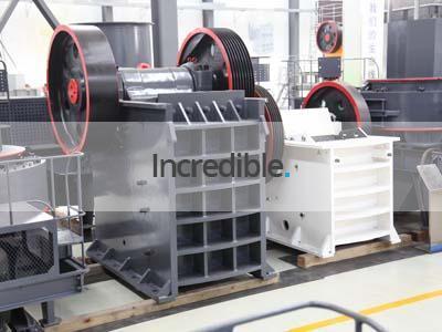
Incredible has successfully built lots of crushing plants, grinding plants and metal ore dressing plants for our customers.
With over 30 years of experience, we become a renowned manufacturer in the stone crushing and mineral grinding industry. Headquartered in Shanghai, China, our expansive factory spans over 120 hectares, empowering us to cater to the production demands of global customers.